
Semiconductor Electronics: Materials, Devices and Simple Circuits | CBSE Class 12 Physics Notes
On this page
Watch & explore
Start with a few high-quality watches, then dive into the notes below.
This note covers semiconductor materials, energy bands, intrinsic and extrinsic semiconductors, electrons and holes, doping, p-n junction formation, forward and reverse bias, diode characteristics, dynamic resistance, half-wave and full-wave rectification, and capacitor filtering.
What distinguishes semiconductors from metals and insulators?
Semiconductors have electrical conductivity intermediate between that of metals and insulators. Their usefulness comes from the possibility of controlling the number and movement of charge carriers. Light, heat or a small applied voltage can change the number of mobile charges within the material.
Conductivity and resistivity
Resistivity, denoted by , measures a material's opposition to electrical conduction. Conductivity, denoted by , is its reciprocal:
The SI unit of resistivity is the ohm metre, . The SI unit of conductivity is the siemens per metre, . A high conductivity corresponds to a low resistivity.
| Material class | Approximate resistivity range | Conduction behaviour |
|---|---|---|
| Metals | to | Low resistivity and high conductivity |
| Semiconductors | to | Intermediate conduction behaviour |
| Insulators | to | High resistivity and low conductivity |
Note: These ranges indicate orders of magnitude. Actual values can lie outside them, and resistivity alone does not explain all differences between the three classes.
Materials and solid-state devices
Silicon and germanium are elemental semiconductors. Compound inorganic examples include gallium arsenide and cadmium sulphide. Organic semiconductors and semiconducting polymers also exist, but silicon and germanium provide the basic models for understanding conduction and junction behaviour.
In a solid-state device, charge carriers are supplied and move within the solid. Semiconductor devices need neither a large evacuated space nor an externally heated cathode. They are small, consume low power, operate at low voltages, and have long life and high reliability.
These features distinguish them from vacuum-tube devices, in which electrons from a heated cathode travel through an evacuated space. The central physical question is therefore how a solid supplies mobile carriers and how their flow can be controlled.
How do energy bands explain electrical conduction?
When atoms form a solid, neighbouring atoms affect the energies available to electrons. Closely spaced allowed energy levels form energy bands. The valence band contains the valence-electron energy levels; the conduction band lies above it in a semiconductor.
Band edges and the energy gap
Let denote the lowest conduction-band energy and the highest valence-band energy. The energy gap, , is their separation:
A band diagram represents electron energies. It does not show the valence and conduction bands occupying separate physical layers inside the crystal. The band edges mark the limits of allowed energies.
| Class | Band structure | Consequence |
|---|---|---|
| Metal | Partially filled bands or overlapping valence and conduction bands | Electrons have accessible states for conduction |
| Insulator | Large gap, broadly | Ordinary thermal excitation cannot readily bridge the gap |
| Semiconductor | Small finite gap, broadly | Some electrons enter the conduction band at room temperature |
The energy unit means electron volt. Representative gaps are about for diamond, for silicon and for germanium. Thus, sharing four valence electrons does not imply identical electrical behaviour.
What the figure shows
Energy bands of different solids
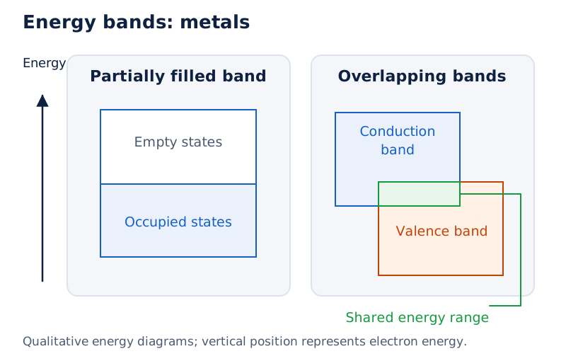
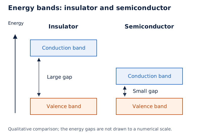
The metal panels show partially filled or overlapping bands. The insulator panel has a large separation between the valence and conduction bands; the semiconductor panel has a smaller separation. The vertical direction represents electron energy.
Drawn by One Young India. See Fig. 14.2 in your NCERT textbook
The temperature condition matters
At absolute zero, silicon and germanium have a filled valence band and an empty conduction band. An intrinsic semiconductor then behaves like an insulator. At higher temperatures, some electrons gain enough energy to cross the gap, leaving vacancies in the valence band.
Conduction can therefore involve both electrons in the conduction band and vacancies in the valence band. Explaining a semiconductor requires both the gap and the availability of carriers, rather than merely calling its resistance intermediate.
How do electrons and holes conduct in an intrinsic semiconductor?
An intrinsic semiconductor is a pure semiconductor. In crystalline silicon or germanium, each atom shares electrons with four nearest neighbours. The shared pairs form covalent bonds, giving the diamond-like crystal structure.
Generation of an electron-hole pair
At low temperatures, the idealised bonding picture has all bonds intact. As temperature rises, some electrons receive sufficient thermal energy to leave their bonds. Each released conduction electron leaves a vacancy called a hole.
Let be the positive magnitude of the electronic charge. The electron has charge , while a hole has effective charge . A hole behaves as an apparent positively charged carrier; it is not a separate positive ion travelling through the lattice.
Let denote the number of conduction electrons per unit volume, the number of holes per unit volume, and the intrinsic carrier concentration. Pair generation gives:
The SI unit of carrier concentration is the reciprocal cubic metre, . These symbols represent concentrations, so they must not be mistaken for total numbers in a sample of unspecified volume.
How a hole moves
- A thermally excited electron leaves a hole at one bond site.
- A bound electron from a neighbouring bond moves into that vacancy.
- The neighbouring bond now has the vacancy, so the hole has apparently moved in the opposite direction.
- The initially freed conduction electron moves independently of this sequence of bound-electron transfers.
What the figure shows
Electron generation and hole motion
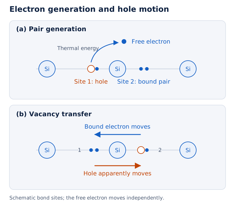
Panel (a) shows a thermally generated free electron and a hole at site 1. Panel (b) shows an electron moving from site 2 towards site 1 and the hole apparently moving towards site 2.
Drawn by One Young India. See Fig. 14.5 in your NCERT textbook
Let be total current, the conventional current contribution from electrons and the contribution from holes. Both contribute to conduction:
The SI unit of electric current is the ampere, . Under an applied electric field, holes move towards negative potential. Electron-hole recombination occurs alongside generation; at equilibrium, the two rates are equal.
How does doping produce n-type and p-type semiconductors?
Doping is the deliberate addition of a small amount of a suitable impurity to a pure semiconductor. The resulting extrinsic semiconductor has much greater conductivity. The impurity atoms, called dopants, replace a small proportion of the original atoms.
A suitable dopant should not substantially distort the original lattice. Its atomic size should therefore be nearly the same as that of the semiconductor atom it replaces. The number of valence electrons determines the carrier type it principally supplies.
Donor impurities and n-type material
A pentavalent dopant, such as arsenic, antimony or phosphorus, has five valence electrons. Four participate in bonds with neighbouring silicon or germanium atoms. The fifth is weakly bound and can become free at room temperature.
The dopant is called a donor. The energy needed to release this extra electron is about in germanium or in silicon, much smaller than the corresponding intrinsic band gap.
With suitable doping, electrons become majority carriers and holes become minority carriers. For n-type material, . Holes still arise through thermal generation; n-type does not mean that holes are absent.
Acceptor impurities and p-type material
A trivalent dopant, such as boron, aluminium or indium, supplies only three valence electrons for bonding. The fourth bond has a vacancy. Acceptance of an electron from a neighbouring bond leaves a hole available for conduction.
Such a dopant is an acceptor. Holes become majority carriers and electrons minority carriers, giving . The ionised acceptor has an effective negative charge, whereas an ionised donor has an effective positive charge.
| Feature | n-type | p-type |
|---|---|---|
| Dopant valency | Five | Three |
| Impurity role | Donor | Acceptor |
| Majority carriers | Electrons | Holes |
| Minority carriers | Holes | Electrons |
| Ionised impurity core | Positive | Negative |
Note: Both materials retain overall charge neutrality. The extra mobile-carrier charge is balanced by the opposite charge of the ionised impurity cores. The letters n and p identify majority carriers, not the net charge of the crystal.
Doping also introduces extra energy levels. The donor level, , lies slightly below the conduction-band edge; the acceptor level, , lies slightly above the valence-band edge. A small energy supply can therefore produce carriers.
How are carrier concentrations calculated after doping?
At thermal equilibrium, electron and hole concentrations satisfy . The intrinsic concentration belongs to the material at the relevant temperature. Doping increases one carrier population while enhanced recombination reduces the minority population.
Derivation: Minority-hole concentration in n-type material
Let denote the donor concentration. Assume donors supply the dominant electron population and are effectively ionised under the conditions considered.
- Begin with the equilibrium carrier relation:
- Divide by the non-zero electron concentration:
- When donor electrons dominate, use :
Result: A large donor concentration produces a small minority-hole concentration under these assumptions. The approximation concerns the electron concentration; the equilibrium product relation supplies the hole concentration.
Worked example 1. A silicon crystal contains and is doped with one part per million of pentavalent arsenic. Its intrinsic concentration is . Find the majority-electron concentration, taking each donor to supply one electron.
Answer: Let be the host-atom concentration and the dimensionless dopant fraction.
- Convert the specified fraction:
- Calculate the donor concentration:
- Since this greatly exceeds the intrinsic concentration,
Worked example 2. For an n-type silicon sample in thermal equilibrium, the electron concentration is and the intrinsic concentration is . Find its hole concentration.
Answer: Use the minority-carrier relation, retaining the concentration units during squaring and division.
- Square the intrinsic concentration:
- Substitute into the equilibrium relation:
- Divide coefficients and powers:
The two results describe the same doping case. The much smaller hole concentration does not mean that the crystal is negatively charged: donor-core charge maintains neutrality. It also shows why setting the electron and hole concentrations equal would be incorrect for this doped sample.
How does a p-n junction form a depletion region?
A p-n junction joins p-type and n-type regions within a semiconductor crystal. A region of a p-type silicon wafer can be converted into n-type material through suitable controlled doping. The boundary is the metallurgical junction.
Simply pressing separate p-type and n-type slabs together does not produce a proper junction. Surface roughness prevents continuous contact at the atomic scale, so carriers would encounter a discontinuity rather than a continuous crystal junction.
Diffusion, uncovered ions and drift
- Because electron concentration is greater on the n-side, electrons diffuse towards the p-side. Holes diffuse from the p-side towards the n-side because of their concentration gradient.
- Departing electrons leave immobile positive donor ions near the n-side boundary. Departing holes leave immobile negative acceptor ions near the p-side boundary.
- These layers form a depletion region, depleted of the mobile carriers involved in the initial diffusion. The fixed ions remain in the lattice.
- The space charges create an electric field from the positive n-side layer towards the negative p-side layer. This field drives electrons towards the n-side and holes towards the p-side.
- The resulting drift current opposes diffusion current. As the electric field builds, drift grows until the two currents balance.
What the figure shows
Junction formation and carrier directions
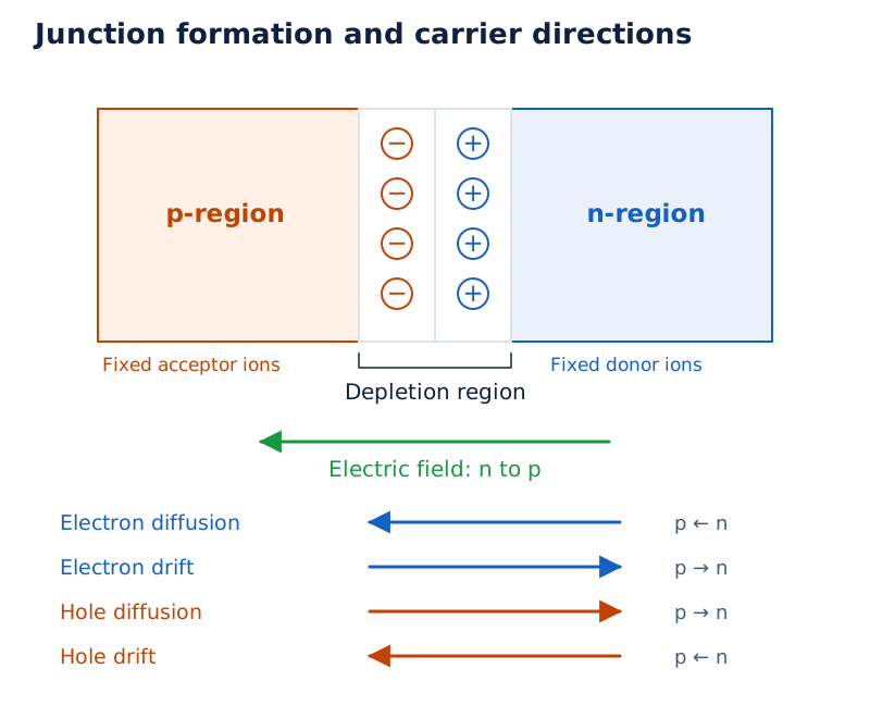
The p-region is drawn on the left and the n-region on the right. Negative and positive fixed charges occupy the narrow junction region. Separate arrows distinguish electron diffusion from electron drift and hole diffusion from hole drift.
Drawn by One Young India. See Fig. 14.10 in your NCERT textbook
Equilibrium and the barrier potential
The junction's built-in barrier potential, denoted by , opposes further majority-carrier diffusion. The n-region is positive relative to the p-region. The SI unit of potential difference is the volt, .
At equilibrium there is no net current, although the opposing drift and diffusion processes balance. It would be incorrect to infer that both processes have stopped. The depletion layer is of the order of one-tenth of a micrometre thick.
The barrier is a consequence of charge redistribution during junction formation. It is already present before an external battery is attached. An applied voltage changes this existing barrier and thereby changes the ease with which carriers cross the junction.
What happens when a diode is forward biased?
A semiconductor diode is a p-n junction with metallic contacts at its ends. These contacts allow an external voltage to be applied, making it a two-terminal device. Its behaviour depends on the polarity of that voltage.
Connections and barrier reduction
For forward bias, connect the p-side to the positive battery terminal and the n-side to the negative terminal. Let denote the magnitude of the applied voltage. Most of this voltage drops across the relatively high-resistance depletion region.
Let denote the effective forward-biased barrier potential. The applied voltage opposes the built-in potential:
The depletion layer narrows and the barrier decreases. With a small applied voltage, relatively few carriers have enough energy to cross. A larger forward voltage lowers the barrier further, allowing more carriers to cross and increasing current.
Minority-carrier injection
- Electrons cross from the n-side into the p-side, where electrons are minority carriers.
- Holes cross from the p-side into the n-side, where holes are minority carriers.
- The minority-carrier concentrations near the junction rise above those farther away on each side.
- Injected electrons and holes diffuse away from their respective junction boundaries, producing forward current.
This process is called minority-carrier injection. The name describes the carriers after they enter the opposite region. It does not mean that the original supply is a large minority population on the side from which they started.
Forward current includes the hole diffusion contribution and the conventional current associated with electron diffusion. Its magnitude is usually in milliamperes. The much smaller drift contribution remains present but is negligible compared with the injected-carrier current.
Note: Forward bias lowers the barrier; it does not justify treating every small forward voltage as producing a large current. The characteristic curve initially rises very slowly before the current increases strongly.
How does reverse bias differ from forward bias?
For reverse bias, connect the n-side to the positive battery terminal and the p-side to the negative terminal. The applied voltage supports the built-in barrier, so the depletion region widens and majority-carrier diffusion is strongly suppressed.
Let denote the effective reverse-biased barrier potential. With again representing the magnitude of the applied voltage:
Why a small reverse current remains
Minority electrons on the p-side and minority holes on the n-side can reach the junction through random motion. The junction field sweeps them into the regions where they are majority carriers. This produces a small reverse current, of the order of microamperes.
Even a small reverse voltage can sweep these carriers across. Their concentration, rather than the voltage magnitude, limits the current. Consequently, the reverse saturation current remains nearly constant with reverse voltage before breakdown.
| Feature | Forward bias | Reverse bias |
|---|---|---|
| Positive battery connection | p-side | n-side |
| Depletion layer | Narrows | Widens |
| Barrier potential | Decreases | Increases |
| Main current mechanism | Injected-carrier diffusion | Minority-carrier drift |
| Typical current scale | Milliamperes | Microamperes before breakdown |
Breakdown and current limits
Let denote the breakdown voltage. When the reverse-voltage magnitude reaches this critical value, a small further voltage increase causes a large current increase. Nearly constant reverse current therefore describes a limited region of the characteristic.
If an external circuit does not limit current below the diode's rated value, overheating can destroy the junction. Excessive forward current can also damage it. General-purpose diodes are operated within their appropriate current and reverse-voltage limits.
How are diode characteristics and resistance interpreted?
A diode's current-voltage characteristic plots current against applied voltage. An adjustable supply allows different readings to be taken. The forward-bias circuit uses a milliammeter, while the reverse-bias circuit uses a microammeter because the expected current is much smaller.
Threshold voltage and dynamic resistance
The forward current is initially very small. Beyond the threshold voltage, or cut-in voltage, it rises strongly even for a small voltage increase. Approximate threshold values are for a germanium diode and for a silicon diode.
Let be dynamic resistance, a small voltage change and the corresponding current change near an operating point. Then:
The SI unit of resistance is the ohm, . Dynamic resistance uses changes between neighbouring points on the curve. It is distinct from the ratio of voltage to current at one point.
What the figure shows
Measuring and plotting diode characteristics
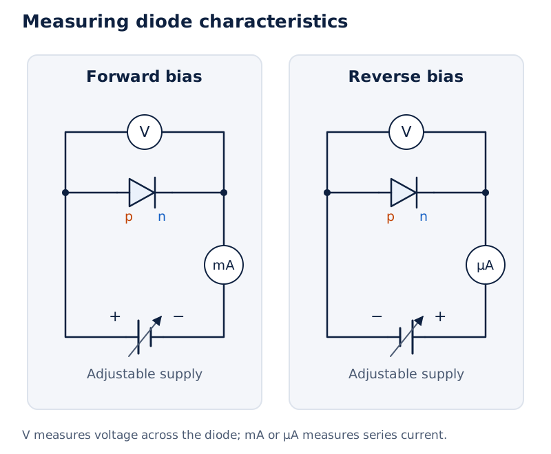
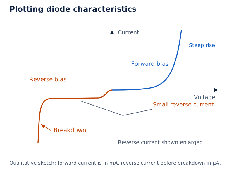
Two circuits show a voltmeter across the diode and an ammeter in series. The forward circuit labels a milliammeter; the reverse circuit labels a microammeter. The graph shows the steep forward rise and the small reverse current before breakdown.
Drawn by One Young India. See Fig. 14.16 in your NCERT textbook
Worked example 3. Near a forward current of , a silicon diode curve passes through at and at . Treat this short segment as straight and find its dynamic resistance.
Answer: Use the changes across the specified segment.
- Find the voltage change:
- Find the current change:
- Calculate the ratio:
Worked example 4. At a reverse voltage of , a diode carries . Find the resistance defined by the voltage-to-current ratio at that point.
Answer: Let denote this point resistance, distinct from dynamic resistance.
- Express the current in amperes:
- Use the signed readings:
- The negative signs cancel:
A correct calculation identifies which resistance is requested and reads the graph's units before substituting. Confusing microamperes with milliamperes would substantially change the result. The large reverse resistance and much smaller forward resistance explain the diode's usefulness for rectification.
How do half-wave and full-wave rectifiers work?
Rectification converts an alternating voltage into an output restricted to one direction. A diode conducts readily during forward bias and offers very high resistance during reverse bias. Rectifier circuits use this difference to select the conducting parts of an alternating input.
Half-wave rectification
A half-wave rectifier has a diode in series with a load resistor. Let denote the load resistance. In the transformer-fed circuit, terminal A becoming positive relative to B forward biases the diode and produces current through the load.
When A becomes negative, the diode is reverse biased and load current is negligible. Output appears during alternate half-cycles only. The diode's reverse breakdown voltage must be sufficiently above the peak secondary voltage.
What the figure shows
Half-wave rectifier and waveforms
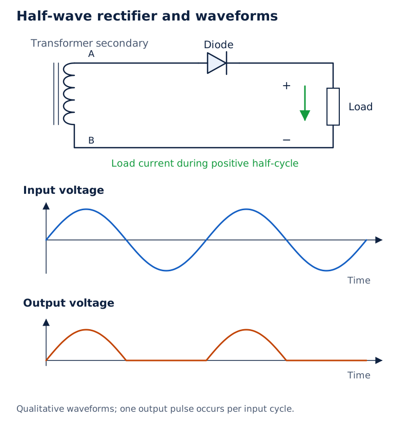
A transformer secondary feeds a diode and load resistor. The input trace alternates above and below its axis; the output trace contains positive half-wave pulses with zero-output intervals between them.
Drawn by One Young India. See Fig. 14.18 in your NCERT textbook
Worked example 5. A half-wave rectifier receives an alternating input of frequency . Find the repetition frequency of its output pulses.
Answer: Let be input frequency and output-pulse frequency.
- One output pulse occurs per complete input cycle, so
- Substitute the given frequency:
Centre-tapped full-wave rectification
A full-wave rectifier can use two diodes and a centre-tapped transformer. The p-sides of the diodes connect to the secondary ends. Their n-sides join, and the load connects between that common point and the centre tap.
- When secondary end A is positive relative to the centre tap, end B is negative.
- The diode at A conducts, while the diode at B is reverse biased.
- During the next half-cycle, B is positive and its diode conducts while the other diode is reverse biased.
- Both conducting paths produce load current in the same direction, giving output during both halves of the input cycle.
What the figure shows
Centre-tapped full-wave rectifier
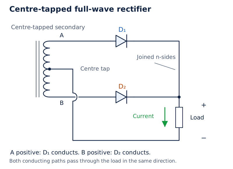
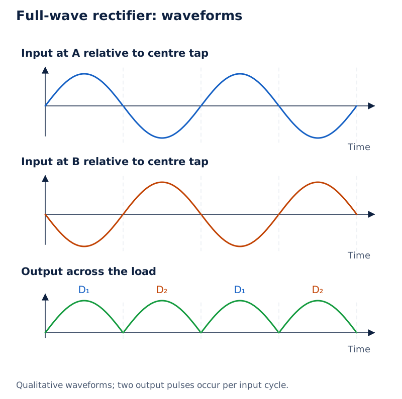
The two secondary ends feed separate diodes whose outputs meet at the load. The centre tap returns to the other load terminal. The two input traces are opposite in phase, and the output contains successive pulses from alternating diodes.
Drawn by One Young India. See Fig. 14.19 in your NCERT textbook
Each diode uses one half of the centre-tapped secondary voltage. The unfiltered output is still pulsating. Producing output in both half-cycles does not make its instantaneous voltage constant.
Derivation: Full-wave output frequency
Let denote the input period and the interval between successive output pulses.
- The input period is the reciprocal of input frequency:
- Two pulses occur per input cycle:
- Taking the reciprocal gives
Result: The full-wave pulse frequency is twice the input frequency. This refers to pulse repetition in the rectified output.
Worked example 6. A full-wave rectifier receives an alternating input of . Find the repetition frequency of its output pulses.
Answer: Both input half-cycles contribute an output pulse.
- Use the full-wave frequency relation:
- Substitute and calculate:
How does a capacitor filter smooth the rectified output?
The output of a rectifier is unidirectional but varies with time. A filter reduces this variation, or ripple. A common arrangement places a capacitor across the output terminals, in parallel with the load resistor.
Charging and discharging
As the rectified voltage rises, the capacitor charges. Without an external load it remains charged to the peak voltage. With a load attached, it discharges through that load as the rectified voltage falls, helping maintain the output between peaks.
The capacitor charges again when the next rectified pulse rises sufficiently. Repeated charging and discharging therefore produces an output nearer the peak rectified voltage, with much less variation than the unfiltered pulses.
What the figure shows
Capacitor smoothing
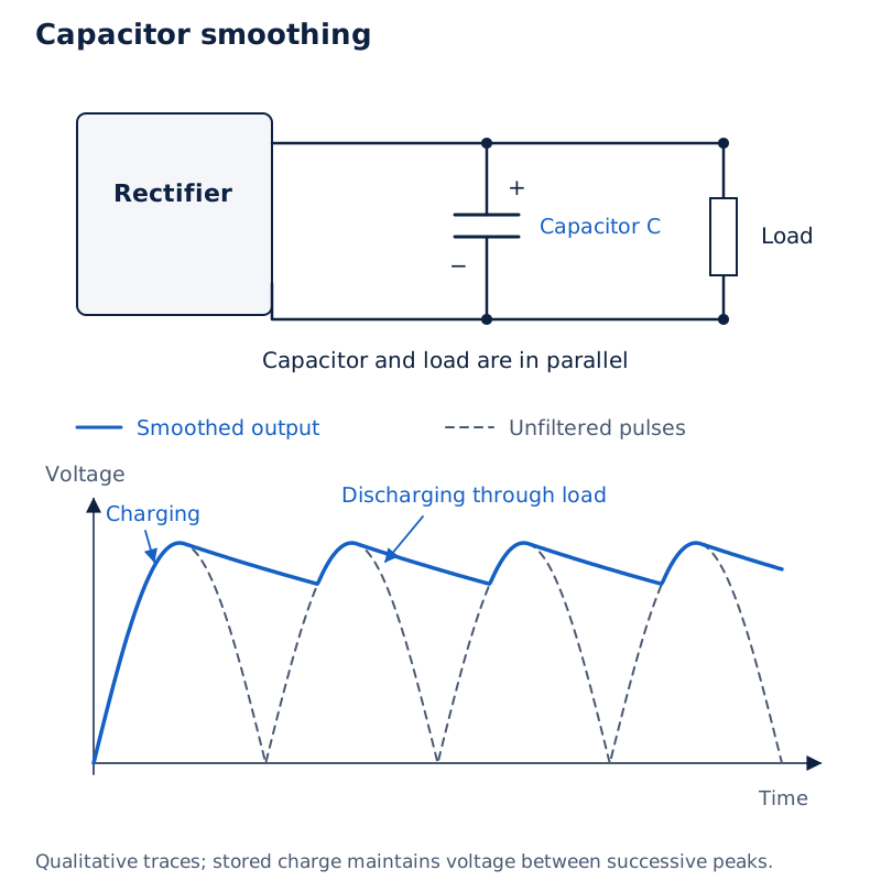
The capacitor is drawn across the rectifier output beside the parallel load resistor. The output trace rises towards successive peaks and falls more gradually between them, rather than returning to zero with every rectified pulse.
Drawn by One Young India. See Fig. 14.20 in your NCERT textbook
The role of the time constant
Let denote capacitance and the circuit's time constant. With effective load resistance , the relevant product is:
A larger product makes the voltage fall more slowly during discharge. Large capacitors are therefore used in capacitor-input filters. The smoothed output is nearer the peak value, but filtering and rectification remain distinct operations: rectification establishes one direction, while filtering reduces variation.
An inductor in series with the load can also serve a filtering purpose. For the capacitor arrangement, the essential points are the parallel connection, charge storage near peaks, and discharge through the load between charging intervals.
Glossary
- Semiconductor — A material with conduction behaviour intermediate between metals and insulators, whose mobile-carrier population can be controlled.
- Valence band — The band containing valence-electron energy levels, filled in an intrinsic semiconductor at absolute zero.
- Conduction band — The higher band whose electrons can move through the solid and contribute to electrical conduction.
- Energy gap — The separation between the highest valence-band energy and the lowest conduction-band energy in a semiconductor.
- Hole — An electron vacancy in a bond that behaves as an apparent carrier of positive electronic charge.
- Intrinsic semiconductor — A pure semiconductor in which the electron and hole concentrations are equal at thermal equilibrium.
- Doping — Deliberate addition of a small amount of suitable impurity to change a semiconductor's carrier concentration and conductivity.
- Donor — A pentavalent impurity in silicon or germanium that supplies an extra electron for electrical conduction.
- Acceptor — A trivalent impurity in silicon or germanium that accepts an electron and supplies a hole for conduction.
- Depletion region — The junction region depleted of mobile carriers, containing fixed ionised donors and acceptors that create an electric field.
- Barrier potential — The built-in potential difference across a junction that opposes further diffusion of majority charge carriers.
- Dynamic resistance — The ratio of a small voltage change to the corresponding current change near a diode's operating point.
- Rectification — Conversion of an alternating voltage into an output voltage restricted to one direction, though it may still pulsate.
- Capacitor filter — A capacitor connected across a rectifier's load to reduce output variation through repeated charging and discharging.
Common errors and misconceptions
- Misconception: An n-type crystal has a net negative charge. Correct: It remains neutral overall because positive donor-core charges balance the additional mobile electrons.
- Misconception: A p-type semiconductor contains no electrons. Correct: Electrons remain as minority carriers; holes are the majority carriers.
- Misconception: A moving hole is a positive ion moving between lattice sites. Correct: Hole motion describes the shifting vacancy as bound electrons move between bonds.
- Misconception: The depletion region contains no charge of any kind. Correct: It contains fixed ionised donor and acceptor cores, although mobile carriers are depleted.
- Misconception: Zero current in an unbiased junction means diffusion and drift both stop. Correct: Their opposing current contributions balance at equilibrium.
- Misconception: Reverse bias produces exactly zero current at every voltage. Correct: A small minority-carrier current flows before breakdown, where reverse current increases sharply.
- Misconception: Dynamic resistance is found by dividing one voltage reading by its current reading. Correct: It uses small changes between nearby points; the single-point ratio is a different resistance.
- Misconception: Full-wave rectification alone provides a constant output voltage. Correct: Its output still pulsates; a filter reduces this variation.
Exam-style questions with model answers
Q1. What is a hole, and how does it move in a semiconductor? [2 marks]
- A hole is an electron vacancy in a covalent bond with an effective positive electronic charge.
- When a neighbouring bound electron fills the vacancy, it leaves a vacancy at its former site. The apparent hole movement is opposite to that electron's movement.
Q2. Compare n-type and p-type silicon in terms of dopants, majority and minority carriers, and overall charge. [3 marks]
- n-type silicon uses pentavalent donor impurities such as arsenic. Electrons are its majority carriers and holes its minority carriers.
- p-type silicon uses trivalent acceptor impurities such as boron. Holes are its majority carriers and electrons its minority carriers.
- Both crystals remain electrically neutral overall. Positive ionised donor cores balance extra electrons in n-type material, while negative ionised acceptor cores balance holes in p-type material. The carrier labels do not specify a net crystal charge.
Q3. Explain the formation of the depletion region and barrier potential in an unbiased p-n junction. Why is its equilibrium net current zero? [5 marks]
- Electron concentration is higher on the n-side, so electrons diffuse towards the p-side. Hole concentration is higher on the p-side, so holes diffuse towards the n-side. These concentration gradients produce diffusion.
- Electrons leaving the n-side uncover immobile positive donor ions. Holes leaving the p-side uncover immobile negative acceptor ions. Together these charged layers form the depletion region.
- An electric field develops from the positive n-side layer towards the negative p-side layer. It drives electrons towards the n-side and holes towards the p-side, producing drift current opposite to diffusion current.
- The separated space charges produce a barrier potential, with the n-side positive relative to the p-side, that opposes further majority-carrier diffusion.
- As the field builds, drift current grows until it balances diffusion current. The net current is zero because opposing currents balance, rather than because all carrier motion ceases.
Q4. A silicon crystal contains and is doped with one part per million of arsenic. Its intrinsic carrier concentration is . Assuming each donor supplies one electron and donor electrons dominate, calculate electron and hole concentrations at thermal equilibrium. [4 marks]
- Let be donor concentration and , , and be electron, hole, and intrinsic concentrations respectively. The dimensionless dopant fraction is
- The donor and approximate electron concentrations are
- The thermal-equilibrium relation gives
- The donor-electron approximation is justified because the donor concentration greatly exceeds the intrinsic concentration. Electrons are therefore majority carriers and holes minority carriers; these answers are numbers per unit volume, not total particle counts.
Q5. A silicon diode carries at and at . Assuming the characteristic is straight over this short interval, calculate its dynamic resistance near and explain the ratio used. [3 marks]
- Let and be the voltage and current changes. Then
- The corresponding current change is
- Dynamic resistance, denoted by , is
- The calculation uses two neighbouring points because dynamic resistance concerns the local change of current with voltage. Dividing a single voltage reading by its current would instead calculate a point resistance.
Q6. Describe a two-diode, centre-tapped full-wave rectifier. Explain the current path in each half-cycle and why a capacitor across the load smooths its output. [5 marks]
- The p-sides of the two diodes connect to opposite ends of the transformer secondary. Their n-sides join, and the load is connected between this common point and the secondary's centre tap.
- Call the secondary ends A and B. When A is positive relative to the centre tap, conventional current flows from A through its forward-biased diode, through the load to the centre tap, and back through that half of the secondary. The diode at B is reverse biased.
- In the next half-cycle, B is positive. Current flows from B through its forward-biased diode, through the load to the centre tap, and back through the other half of the secondary. The diode at A is reverse biased. Load current has the same direction in both half-cycles.
- The output contains pulses from both halves of the alternating input and remains unidirectional but pulsating. A capacitor in parallel with the load charges near the peaks when the rectified voltage exceeds its stored voltage.
- Between charging intervals, the capacitor discharges through the load, helping maintain the output voltage and reducing its variation.
Q7. A half-wave rectifier and a full-wave rectifier each receive a alternating input. Calculate their output-pulse frequencies. [2 marks]
- Half-wave rectification supplies one pulse per complete input cycle. Its output frequency is where denotes the half-wave output-pulse frequency.
- Full-wave rectification supplies two pulses per complete cycle. Its output frequency, , is
Q8. Explain why reverse current is small and nearly voltage independent before breakdown, and state what happens at breakdown. [3 marks]
- Reverse bias widens the depletion region and increases the barrier, strongly suppressing majority-carrier diffusion.
- The junction field sweeps minority electrons and holes across when they reach the junction. Their small concentrations limit the current; even a small reverse voltage is sufficient to sweep them across.
- The reverse current therefore remains nearly constant before breakdown. At the breakdown voltage it rises sharply. Unless the external circuit limits current below the rated value, overheating can destroy the diode.
Key takeaways
- Energy-band structure and the availability of mobile carriers explain the contrasting electrical behaviour of metals, semiconductors and insulators.
- Intrinsic semiconductors produce electrons and holes in equal concentrations; both carrier types contribute to electrical current.
- Pentavalent donors produce n-type silicon or germanium, while trivalent acceptors produce p-type material; both remain neutral overall.
- A p-n junction develops fixed space charges, a depletion region and a barrier potential as drift balances diffusion.
- Forward bias reduces the barrier and injects carriers; reverse bias raises the barrier and leaves a small minority-carrier current.
- Dynamic resistance uses nearby voltage and current changes, while a point resistance uses the voltage and current at one operating point.
- A half-wave rectifier uses alternate half-cycles; a full-wave rectifier uses both half-cycles and doubles the output-pulse frequency.
- A capacitor across the load reduces rectified-output ripple by charging near peaks and discharging through the load between them.
Test yourself
Why does an intrinsic semiconductor behave like an insulator at absolute zero?
Its valence band is filled and its conduction band is empty, so thermally generated conduction electrons and holes are absent.
Which carriers are the minority carriers in n-type and p-type materials?
Holes are minority carriers in n-type material, while electrons are minority carriers in p-type material.
Why does donor doping not give the whole crystal a negative charge?
The ionised donors leave positive fixed cores that balance the charge of the additional mobile electrons.
What distinguishes diffusion from drift at a junction?
Diffusion results from a carrier concentration gradient. Drift is carrier motion caused by an electric field.
Which battery connections forward bias a p-n junction diode?
The p-side connects to the positive terminal, and the n-side connects to the negative terminal.
Why is a microammeter used when measuring ordinary reverse-bias current?
The current is much smaller than typical forward current and is of the order of microamperes.
Does a full-wave rectifier's unfiltered output have a constant value?
No. It has one direction but still consists of pulses; filtering is needed to reduce the variation.
Where is a capacitor connected when it is used to smooth a rectifier's output?
It is connected across the output terminals, in parallel with the load, so it can discharge through the load.